课程名称 课程工具 官网资源 软件安装 原理图设计 原理图实例 印制板图设计 器件的封装 PCB实例 实物展示(菲林、钢网)
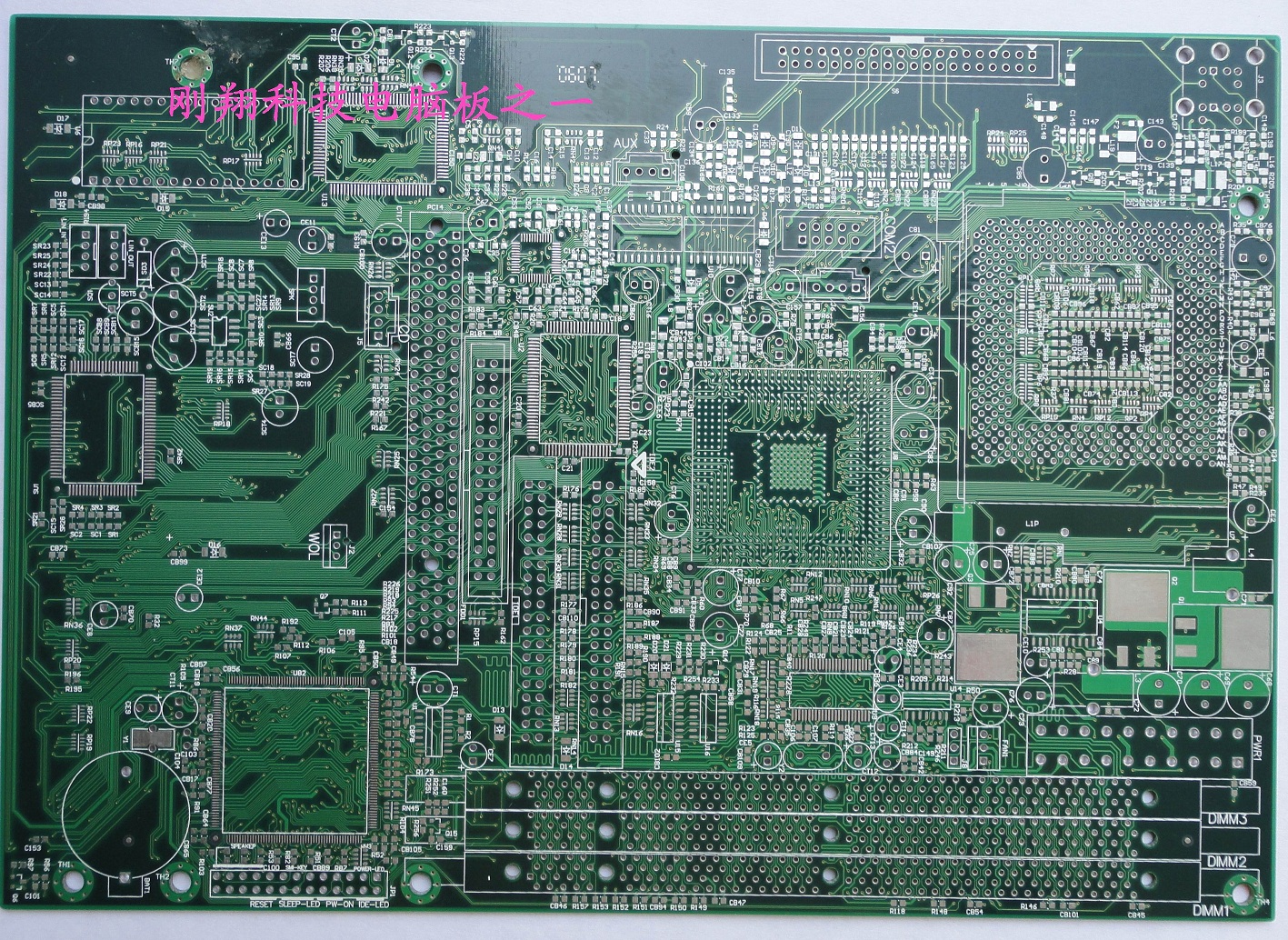
印刷电路板Printed circuit board
A printed circuit board (PCB) mechanically supports and electrically connects electronic components using conductive tracks, pads and other features etched(蚀刻) from copper sheets laminated(由薄片叠成的) onto a non-conductive substrate(基底). PCBs can be single sided (one copper layer), double sided (two copper layers) or multi-layer (outer and inner layers). Multi-layer PCBs allow for much higher component density. Conductors on different layers are connected with plated-through holes called vias. Advanced PCBs may contain components - capacitors, resistors or active devices - embedded in the substrate.
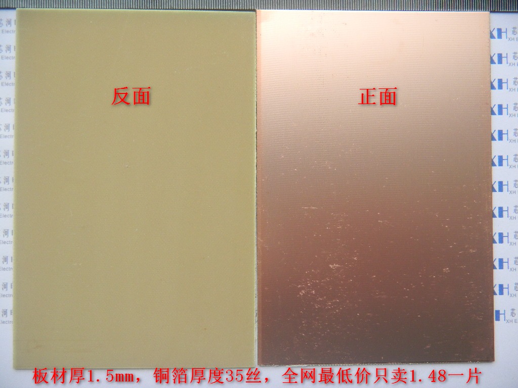
印制电路板原材料:单面玻纤覆铜板
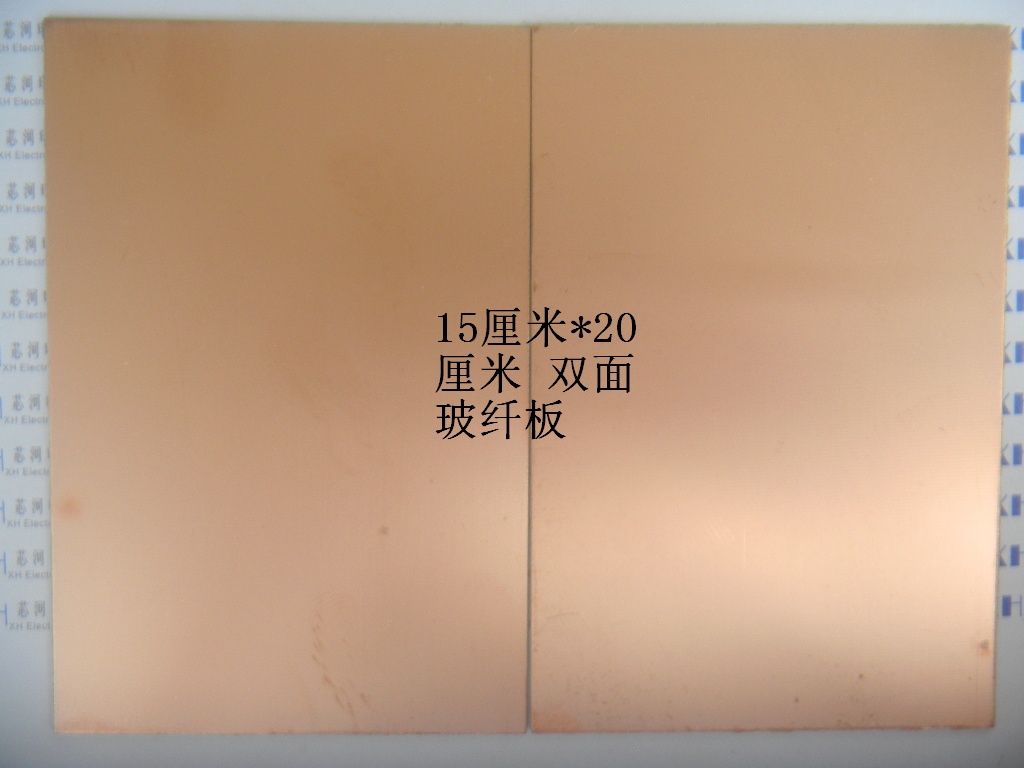
印制电路板原材料:双面玻纤覆铜板
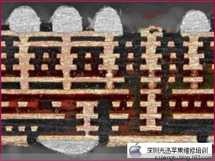
iphone4印制板刨面图