Nios II processor architecute
(from:Nios II Classic Processor Reference Guide)
1、Register File
The Nios II architecture supports a flat register file, consisting of thirty-two 32-bit general-purpose integer registers, and up to thirty-two 32-bit control registers.
The architecture supports supervisor and user modes that allow system code to protect the control registers from errant applications.
The Nios II processor can optionally have one or more shadow register sets. A
shadow register set is a complete set of Nios II general-purpose registers. When
shadow register sets are implemented, the
CRS field of the status register indicates which register set
is currently in use. An instruction access to a general-purpose register uses
whichever register set is active.
A typical use of shadow register sets is to accelerate context switching. When
shadow register sets are implemented, the Nios II processor has two special
instructions, rdprs and wrprs, for moving data between register sets. Shadow
register sets are typically manipulated by an operating system kernel, and are
transparent to application code. A Nios II processor can have up to 63 shadow
register sets.
The Nios II architecture allows for the future addition of
floating-point registers. For details about shadow register set implementation
and usage, refer to “Registers” and “Exception
Processing” in the
Programming Model chapter of the Nios II Processor Reference Handbook.
For details about the rdprs and wrprs instructions, refer to the Instruction
Set Reference chapter of the Nios II Processor Reference Handbook.
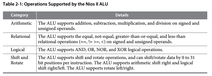
2、Arithmetic Logic Unit
The Nios II ALU operates on data stored in general-purpose
registers. ALU operations take one or two inputs from registers, and store a
result back in a register. The ALU supports the data operations described in the
table below. To implement any other operation, software computes the result by
performing a combination of the fundamental operations.

3、Custom Instructions
from:Nios II Custom Instruction user guide.pdf
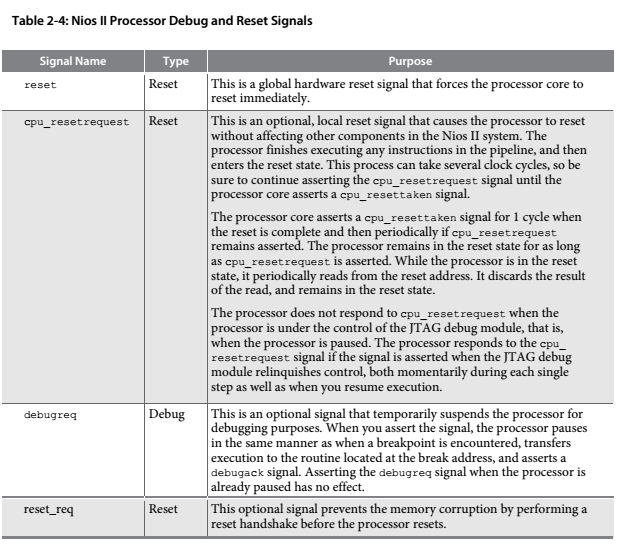
Reset and Debug Signals
The table below describes the reset and debug signals that the Nios II processor
core supports.

4、5、Exception and Interrupt Controllers
The Nios II processor includes hardware for handling exceptions, including
hardware interrupts. It also
includes an optional external interrupt controller (EIC) interface. The EIC
interface enables you to speed
up interrupt handling in a complex system by adding a custom interrupt
controller.
6、7、instruction and data bus
from:Nios II Gen2 Processor Reference Guide
The Nios II architecture supports separate instruction and data buses, classifying it as a Harvard architecture. Both the instruction and data buses are implemented as Avalon-MM master ports that adhere to the Avalon-MM interface specification. The data master port connects to both memory and peripheral components, while the instruction master port connects only to memory components.
Note:
The Nios II instruction and data masters have a combined address map. The memory model is arranged so that instructions and data are in the same address space.
8、Memory Management Unit
9、Memory Protection Unit
When present and enabled, the MPU monitors all Nios II instruction fetches and data memory accesses to protect against errant software execution. The MPU is a hardware facility that system software uses to define memory regions and their associated access permissions. The MPU triggers an exception if software attempts to access a memory region in violation of its permissions, allowing you to intervene and handle the exception as appropriate. The precise exception effectively prevents the illegal access to memory.
The MPU extends the Nios II processor to support user mode and supervisor mode. Typically, system software runs in supervisor mode and end-user applications run in user mode, although all software can run in supervisor mode if desired. System software defines which MPU regions belong to supervisor mode and which belong to user mode.
11、Tightly-Coupled Memory
The Nios II/f core provides optional tightly-coupled memory interfaces for both instructions and data.
A Nios II/f core can use up to four each of instruction and data tightly-coupled memories. When a tightly-coupled memory interface is enabled, the Nios II core includes an additional memory interface master port. Each tightly-coupled memory interface must connect directly to exactly one memory slave port.
When tightly-coupled memory is present, the Nios II core decodes addresses internally to determine if requested instructions or data reside in tightly-coupled memory. If the address resides in tightly-coupled memory, the Nios II core fetches the instruction or data through the tightly-coupled memory interface. Software accesses tightly-coupled memory with the usual load and store instructions, such as ldw or ldwio.
Accessing tightly-coupled memory bypasses cache memory. The processor core functions as if cache were not present for the address span of the tightly-coupled memory. Instructions for managing cache, such as initd and flushd, do not affect the tightly-coupled memory, even if the instruction specifies an address in tightly-coupled memory.
When the MMU is present, tightly-coupled memories are always mapped into the kernel partition and can only be accessed in supervisor mode.
12、JTAG Debug Module
The Nios II architecture supports a JTAG debug module that provides on-chip
emulation features to
control the processor remotely from a host PC. PC-based software debugging tools
communicate with the
JTAG debug module and provide facilities, such as the following features:
• Downloading programs to memory
• Starting and stopping execution
• Setting breakpoints and watchpoints
• Analyzing registers and memory
• Collecting real-time execution trace data
